Blue Robotics - Electronics Design Co-Op
My main project as a co-op at Blue Robotics was to improve the speeds of the tethered communications used for the ROVs. This involves implementing G.hn technology into the PCBs in the ROVs, allowing for Gigabit, 100Base-T and 10Base-T communication with connected devices. This project involved the design of multiple boards.
The Gigaboard 


This is the main board used in the ROVs. This board was a very intricate six-layer project, which bridges G.hn data over the tether to multiple Ethernet PHYs using multiple forms of MII connections and multiple Ethernet switch controllers. The board also acts as a flight controller, complete with all necessary signals and connections, along with an STM32H5. The design includes:
- A G.hn processor, which connected to the tether. This processor is connected to two analog front-end chips which modulates the digital data from the processor into analog data, and demodulates the analog data received back to digital data for the processor to read. This subcircuit has impedance matched traces and Ethernet magnetics for protection.
- A Gigabit Ethernet PHY interfaced to the G.hn processor via RGMII and to an Ethernet switch via a Gigabit connection. This PHY provides the physical layer interface between the processor and switch that allows them to communicate.
- Two Ethernet Switch Controllers. These allow the user to interface a device to the ROV with a Gigabit or 100Base-T Ethernet connection via an RJ45 or wire-to-board connectors. These switches are also interfaced to three 10Base-T PHYs and an STM32H5 via MII. These subcircuits have impedance matched differential pair traces and Ethernet magnetics.
- Three 10Base-T PHYs, allowing the user to interface a device to the ROV with a 10Base-T Ethernet connection. These subcircuits are complete with ESD protection.
- An STM32H5 microcontroller, interfaced with an Ethernet Switch via MII to establish Ethernet connection between the two. The MCU is also utilizes four SPI and two I2C buses, a USART bus for programming, four ADCs, and is connected to many more peripherals.
- Four buck converters and an LDO, along with reverse polarity protection.
- For flight controller capabilities, the board contains:
- Eight PWM outputs connected to the MCU.
- An IMU connected over SPI. Two magnetometers, one over SPI and one over I2C.
- Current and voltage sense, connected to the ADCs of the MCU.
- Two leak sensor connections, an external fan connection, external voltage and power switch connections, along with an extra ADC and I2C connection.


Switch Testing Board 


- This board was used to test the interfacing of G.hn from the tether to the ROV. The design includes:
- An Ethernet Switch Controller. This was the main chip being tested, seeing if devices could be interfaced with a Gigabit or 100Base-T Ethernet connection through a G.hn interface. This chip has impedance matched differential pair traces and Ethernet magnetics.
- A 10Base-T PHY connected to the Switch, testing if a 10Base-T connection could be established through a G.hn interface.
- External connectors for I2C and SPI access to the Switch.
- 24 pin connectors to test Switch-to-Switch communication between two boards.


Paradigm Engineering - Team Lead & Electrical Designer
Paradigm Engineering is the largest design and competition team at the Memorial University of Newfoundland. The team has competed at the SpaceX Hyperloop Pod Competitions, The Boring Company's "Not-a-Boring" competition, and the Intelligent Ground Vehicle competition. Paradigm is gearing up to compete in the Autonomous Karting Series in 2025, creating a fully autonomous, self-driving go-kart.
Control Board 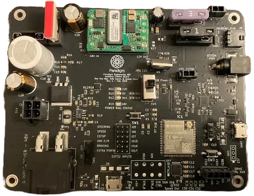
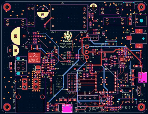
This board interfaces a Pixhawk flight controller to an ESP32 for autonomous motor control. The design includes:
- An ESP32 microcontroller, which processes signals from the Pixhawk flight controller to generate PWM and output signals for motor control. The ESP32 communicates with the Pixhawk via UART and directly drives motor control circuits.
- A USB-to-UART bridge, enabling firmware programming and communication with the ESP32 from a USB-connected laptop. This subcircuit ensures seamless debugging and software updates.
- A bidirectional logic level shifter, converting the ESP32's 3.3V PWM signals to 5V for compatibility with motors requiring 5V input. This ensures reliable signal transmission between the MCU and motor drivers.
- Two USB connectors:
- One connected to the USB-to-UART bridge for programming and communication.
- One directly interfaced with the ESP32 for standalone connectivity.
- Power management circuitry:
- A 48V to 12V buck converter for stepping down the main battery voltage.
- A 12V to 5V linear regulator, followed by a 5V to 3.3V LDO, providing clean power to the ESP32 and peripherals.
- A hot-swap controller with integrated safety features:
- Overcurrent protection via a sense resistor.
- Undervoltage lockout using a voltage divider network.
- A toggle switch for manual system power control.
- Motor output interfaces:
- Two motor channels with fuses for overcurrent protection.
- Flyback diodes across each motor output to suppress voltage spikes from inductive loads.
- A barrel jack connector to power an NVIDIA Jetson device from the 12V rail.


Power Distribution Board 

This board is used to safely and efficiently distribute power from the battery to our auxiliary components. The design includes:
- A hot-swap IC to safely connect and remove the battery connection. The IC is connected to a sense resistor for overcurrent protection, a voltage divider for under-voltage protection, and a switch to toggle the system.
- A 48 to 12-volt buck converter is used as certain components require a 12V input. This specific buck was chosen for efficiency purposes, looking at current draw and power consumption.
- Output connectors. Each connector is connected to a fuse for current protection, and a flyback diode to protect inductive loads from high voltage spikes.


ESP Proof of Concept Board 
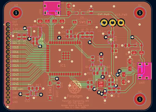
This board is used for testing the functionality of the ESP32 used on the vehicle, which includes the programming of the ESP, and the ability to measure the outputs of the pins. This also allows us to move away from using the ESP32 development kits, giving us freedom in what we include in our design. The board contains:
- A USB to UART bridge, with a USB connector as the input. This allows the ESP to use the code written on the USB-connected laptop via UART.
- The ESP32 microcontroller, which will be used to control the motors on the vehicle.
- A 3V3 linear regulator, providing power to the ESP and ICs on the board.
- An op-amp to boost the ESP output, as some motor function, requires a voltage higher than the 3V3 output.
- A voltage translator is used to raise 3V3 voltage to 5V directly.
- A through-hole header that allows all outputs to connect to an external breadboard for easy testing and use.


Drive Motor Supply Board 

This board is used to safely and efficiently supply power from the battery to our drive motor. The design includes:
- A hot-swap IC to safely connect and remove the battery connection. The IC is connected to a sense resistor for overcurrent protection, a voltage divider for under-voltage protection, and a switch to toggle the system.
- An output connector, connected to a fuse for current protection, and a flyback diode to protect the load from high voltage spikes.


MUNStar-1 - Electrical Power System Designer
MUNStar-1 is a student design team based out of the Memorial University of Newfoundland. Its aim is to create a small satellite, called a CubeSat through the Canadian Space Agency's “CUBICS” Mission. The power subsystem supplies essential DC power to key components. The system includes a timer circuit PCB for a thirty-minute power-off period post-launch, called the inhibitor circuit
Inhibitor Circuit 
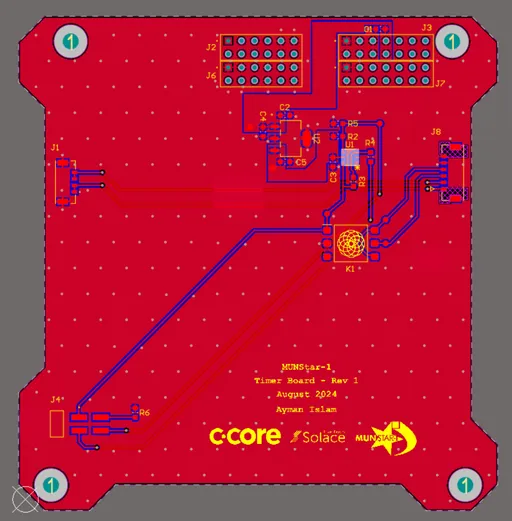
A programmable timer chip, programmed using external resistors. Provides simplicity compared to using a 555 timer and logic circuitry:
- A 5V linear regulator.
- A photorelay for fast switching once the timer outputs the signal.
- A jumper header that switches the timer from 30 minutes to 30 seconds, making the system available for quick testing.
- All components are temperature-rated and vibration-tested for use in space.


F-MUN-TENTH - Electrical Team Member
Created an autonomous racing vehicle to compete in the F1 Tenth competition. Placed top 10 in May 2023 in San Antonio, Texas.
Work Included 

- Soldered PCBs and wired various components.
- Configured a system containing a LiDAR, motor controller, and NVIDIA Jetson GPU.

